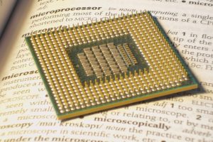
On the right is the processor package from my old laptop. The numbers  associated with microelectronic devices like this one are beyond comprehension. The actual processor – the grey rectangle in the middle – measures only 11 mm by 13 mm and yet, according to the manufacturer, it contains 291 million transistors. That’s about 2 million transistors per square millimetre.
To try to bring these numbers within my comprehension, I asked the following question:
If I were to magnify the processor – the grey rectangle – so that I could just make out the features on its active surface with my unaided eye, how big would it be?
The answer is that the processor would be something like 15 metres across.
Consider that for a moment: an area slightly larger than a singles tennis court, packed with detail so fine that you can only just make it out.
The package that the processor is part of would be over 50 metres across, and the pins on the back of the package (right) would be 3 metres tall, half a metre thick, and about 2 metres apart.
Caveat
The result above is rather approximate, as you’ll see if you read the details of the calculation below. However, if it inadvertently overstates the case for my processor, which is 10 years old, the error is made irrelevant by progress in microprocessor fabrication. Processors are available today that are similar in physical size but on which the features are nearly 5 times smaller. If my processor had that density of features, the magnified version would be around 70 metres across, on a package 225 metres across. And those pins would be 13 metres tall and 2.25 metres thick.
The calculation
The processor is an Intel T7500. According to the manufacturer, the chip is made by the 65-nanometre process. Exactly what this means in terms of the size of the features on the chip is quite hard to pin down. Printed line widths can be as low as 25 nm, but the pitch of successive lines may be greater than the 130 nm that you might expect. I’ve assumed that the lines on the chip and the gaps between them are all 65 nm across.
“The finest detail that we can make out” isn’t well defined either. It depends, among other things, on the contrast. But roughly, the unaided human visual system can resolve details as small as 1 minute of arc subtended at the eye in conditions of high contrast. This is about 3 × 10⁻⁴ radians. At a comfortable viewing distance of 30 cm, this corresponds to 0.09 mm.
So to make the features on the processor just visible (taking high contrast for granted) we need to magnify them from 65 nm to 0.09 mm, which is a magnification factor of 1385.
Applying this magnification factor to the whole processor, its dimensions of 11 by 13 millimetres become 15 by 18 metres. The pins are 2 mm high, so they become 2.8 metres high and about half a metre thick.
Some processors are now made using 14 nm technology. This increases the required magnification factor by a factor of 65/14, to 6430, yielding the results given in Caveat above.